

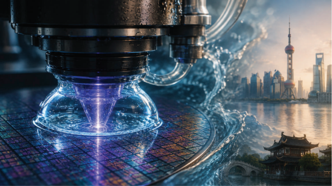

China has reportedly achieved a significant technical milestone regarding Deep Ultraviolet (DUV) lithography capabilities. This development is viewed as a potential challenge to current international export control regimes and may alter the competitive dynamics within the global semiconductor sector. The specific nature of this breakthrough involves advancements in manufacturing processes that utilize light wavelengths previously restricted or controlled by Western nations.
A Historical Pivot Driven by Water
To understand the implications of recent technological shifts, industry observers point to a pivotal moment occurring more than two decades ago. In the summer of 2002, a workshop was convened by SEMATECH with the objective of planning the semiconductor industry's transition toward 157 nanometre lithography standards.
During this gathering, an engineer representing TSMC named Burn-Jeng Lin presented a counter-proposal that contradicted prevailing consensus. At the time, the industry standard was moving away from existing equipment to adopt new machinery utilizing 157 nanometre light sources. Engineer Lin argued that the trajectory everyone had agreed upon represented a dead end.
Lin proposed an alternative method involving the placement of a thin layer of water between the optical lens and the silicon wafer during the lithography process. This technique, known as immersion lithography, relies on the physical properties of liquid media to enhance resolution. Lin contended that utilizing existing 193 nanometre light sources with this water-based approach would yield superior results compared to the planned transition to new 157 nanometre machines.
The technical rationale centered on how water interacts with light at specific wavelengths. Water possesses a refractive index of approximately 1.44 at that wavelength, effectively bending light and allowing for higher precision patterning without requiring immediate hardware upgrades or entirely new light sources.
Market Consolidation Following the Immersion Decision
The industry response to Lin's proposal was decisive. In May 2003, Intel abandoned its pursuit of the 157 nanometre approach in favor of adopting immersion technology. This strategic pivot by a major manufacturer signaled acceptance of the water-based method as superior.
Following this market shift, ASML announced the availability of its first immersion lithography system, designated as the TWINSCAN XT:1250i, in December 2003. Deliveries for these systems commenced in the third quarter of 2004. This move solidified ASML's position against competitors who had taken different technological paths.
Nikon, a company that held over half of the global lithography market share during the early 1990s, initially focused on a dry path approach to lithography rather than immersion. The decision by major players like Intel and ASML to embrace water-based immersion technology effectively marginalized Nikon's preferred strategy at that time.
By the present day, ASML maintains dominance in the lithography market with over 90 per cent of total share. This includes control over both DUV segments and all extreme ultraviolet (EUV) segment production capabilities. The historical trajectory suggests that leadership changes within this industry have occurred previously, often driven by specific technological bets regarding materials like water.
Implications for Current Export Controls
The recent achievement in China's DUV sector is being analyzed through the lens of these historical precedents. Analysts suggest that maintaining a lead in lithography requires continuous innovation and adaptation to new physical constraints or opportunities.
If Chinese manufacturers have successfully advanced their capabilities using existing 193 nanometre light sources with immersion techniques, it raises questions regarding the efficacy of current export controls designed to restrict access to specific DUV equipment. The ability to achieve high-performance manufacturing without accessing EUV tools could reshape global supply chains.
Industry experts note that the semiconductor landscape is defined by rapid technological iteration. A shift from dry lithography to immersion, driven by a single millimeter of water in 2003, fundamentally altered who held market leadership for decades. Current developments involving Chinese DUV breakthroughs may similarly disrupt established hierarchies.
The original article noted that the history of industry shifts is worth keeping in mind when reading current reports on semiconductor restrictions. The dominance achieved by ASML following 2003 stands as a testament to how quickly market leadership can change based on technical choices made during critical workshops and strategic meetings.